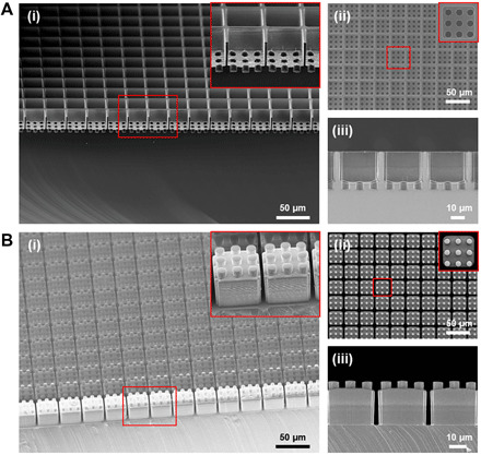
Fig. 2. Fabrication of Si master mold and h-PDMS stamp.

Scanning electron microscopy (SEM) images of the ice cube tray–shaped (A) Si master mold, and (B) h-PDMS stamp showing (i) a tilted view, (ii) a top view, and (iii) a cross-sectional view, respectively. The inset images show a magnified view of the microstructures of the fabricated Si master mold and h-PDMS stamp.
