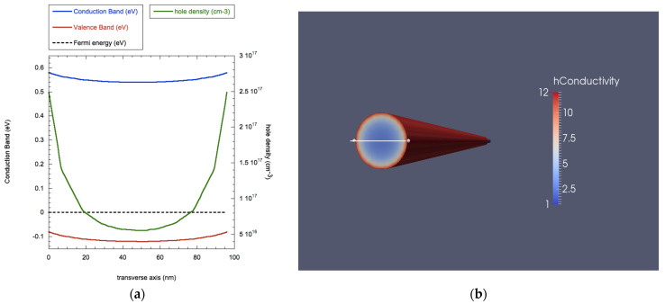
Figure 2.
(a) Values for energy bands (blue: bottom of conduction band, red: peak of valence band), Fermi level (dashed black line) and carrier density (green line) along the trasverse axis; (b) transverse section of a 3D plot of conductivity for a Ge NW. The white line indicates the transverse axis for band profiles.

