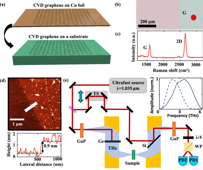
Figure 1.
Sample fabrication and experimental set-up. (a) Schematic of sample fabrication: CVD graphene on Cu foil is transferred onto a desired substrate. (b) 5X optical microscope image of graphene (right section) on SiO2 (left section). (c) Raman spectrum of a transferred graphene film featuring distinctive G and 2D peaks. (d) Atomic force micrograph of graphene transferred on SiO2 together with a height profile across the graphene edge, indicated by the white line. (e) Schematic of the time-domain terahertz spectrometer with its optical components: beam splitter (BS), translation stage (TS), gallium phosphide crystals (GaP), germanium and silicon wafer (Ge and Si), quarter wave plate (QWP), Wollaston prism (WP), and balanced photodetectors (PD).

