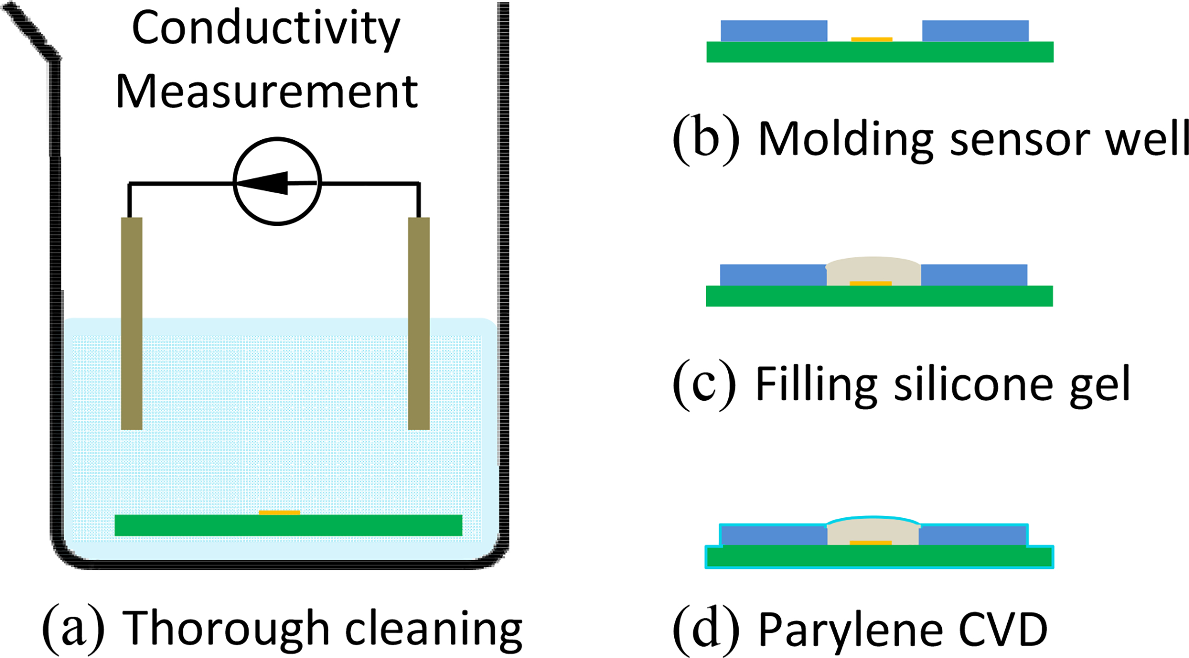
Figure 2:

Main steps of proposed micropackaging process. (a) Thorough cleaning to remove ionic contamination. Conductivity of rinsing solution was characterized as an index of device cleanness. (b) Sensor well was built from PDMS mold. (c) Silicone gel was filled into sensor well and cured with a flat or convex shape. (d) Two 5-μm thick layers of Parylene-C were deposited to protect the soft silicone gel.
