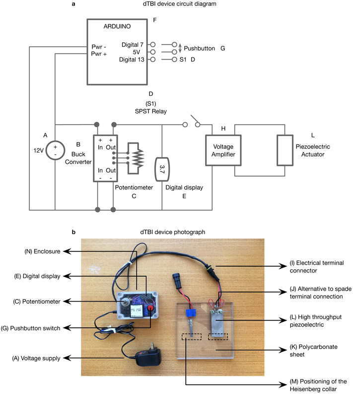
Figure 3. dTBI device overview:
a. Circuit diagram b. Photograph of dTBI device with parts labelled according to the Materials section: A) Voltage supply B) Buck converter C) Potentiometer D) SPST relay E) Digital display F) Arduino G) Pushbutton switch H) Proportional voltage booster I) Electrical terminal connector J) Alternative to spade terminal connection K) Polycarbonate sheet L) Piezoelectric actuator M) dotted lines indicating the positioning of the Heisenberg collar N) Enclosure.
It should be noted that certain minor aspects of this version of the device shown in the photograph in b. are different from the description in the Device Construction section and Fig 4. The openings for the female mount and electrical terminal connector are on the same side of the enclosure, the voltage booster is mounted on top of the enclosure, and the electrical terminal connectors are connected to the piezoelectric wires directly rather than through spade terminals. However, the changes described in the protocol are all designed to increase the robustness or convenience of the design.

