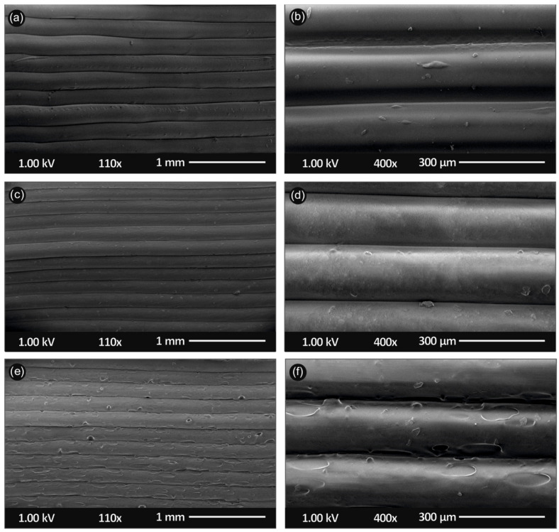
Figure 9.
Scanning electron microscopy (SEM) images of the side-surface microstructure and morphology for the different 3D printed samples in this study at two different magnifications (all 3D printed samples with 300 µm 3D printed layer thickness): SEM images at 110× and 400× magnification for the (a,b) pure PLA, (c,d) PLA/SiO2 (1.0 wt.%) and (e,f) PLA/SiO2 (4.0 wt.%) nanocomposites, respectively.

