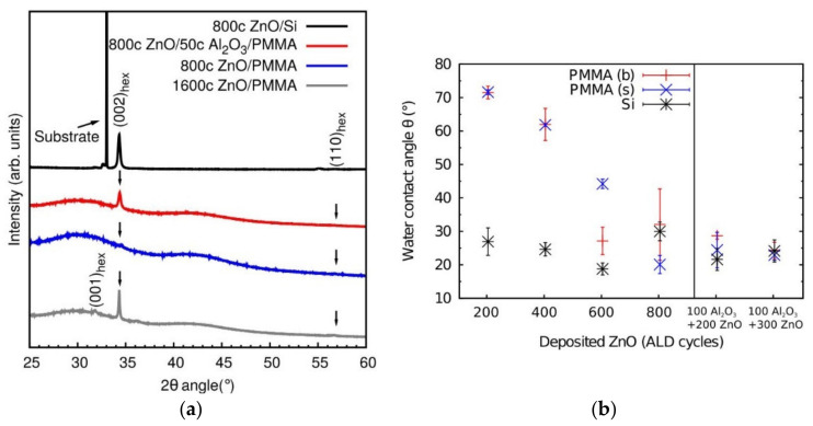
Figure 16.
XRD patterns for 800 cycles of ZnO ALD onto: Si (black) and bulk PMMA substrates with (red) and without Al2O3 seed layer (blue), and an XRD pattern of 1600 cycles ZnO film on bulk PMMA(grey). (a) Water contact angles (θ) of UV-illuminated ZnO deposited on bulk PMMA (red), spin-coated PMMA (blue), and Si substrates as a function of ZnO ALD cycles (black). The two right-most points represent the contact angles of ZnO deposited on 100 cycles Al2O3 intermediate layer (b) (reprinted with permission from [67], Copyright (2014), American Vacuum Society).

