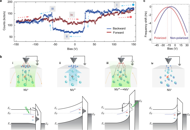
Fig. 4. Schematic model of the charge state control.
a Fluorescence-bias curves over the full-bias range. The dashed arrows denote the direction of bias ramp. b Cartoon graphs (upper panels) and energy band diagrams (lower panels) showing the concerted effect of photon ionization and tip electric field. Upper panels: red and black balls indicate NV_ and NV+ states, respectively. Dashed arrows denote the local electric field. Lower panels: the purple curve denotes the donor’s charge transition level, while blue and red short lines denote NV+/ NV0 and NV0/NV− transition levels, respectively. The waved green arrow denotes exciting photons. EF, EC, and EV denote the Fermi level, conduction, and valence band edges of diamond, respectively. (i) Under a large positive bias, lots of photon-ionized electrons (dark blue balls) from the donors (cyan balls) are driven upward and trapped by the surface defects. (ii) A strong built-in electric field (light blue arrow) remains when the tip is grounded, leading to the upward band bending and the NV+ state. (iii) The surface-trapped electrons are photoexcited and tunnel to the conduction band under negative bias, thence recombined with the donors, depolarizing the surface and leading to the NVˉ state again. (iv) When the bias is grounded again, only shallow donors are depleted due to the electron transfer to surface defects and a small built-in electric field is formed, thus the NV− state remains. c LCPD measurements confirmed the negatively charged surface after polarization. Setpoint: = +20 Hz.

