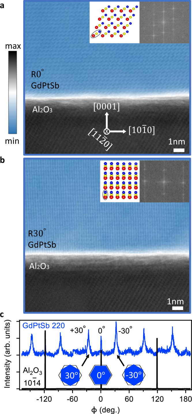
Fig. 3. Heusler/graphene/sapphire interface.

a, b STEM image of the GdPtSb/graphene/Al2O3 interface for the two different GdPtSb domains, as viewed along the zone axis. We used log scale false-color image to simultaneously visualize the film and substrate for better contrast. The insets show the schematic crystal structures and fast Fourier transforms of the STEM images. c In-plane ϕ scan of GdPtSb 220 reflections and Al2O3 104 reflections for GdPtSb sample grown on graphene/Al2O3. Δϕ = ±30° are the in-plane angles between the 〈101〉 direction of GdPtSb and the direction of Al2O3 substrate.
