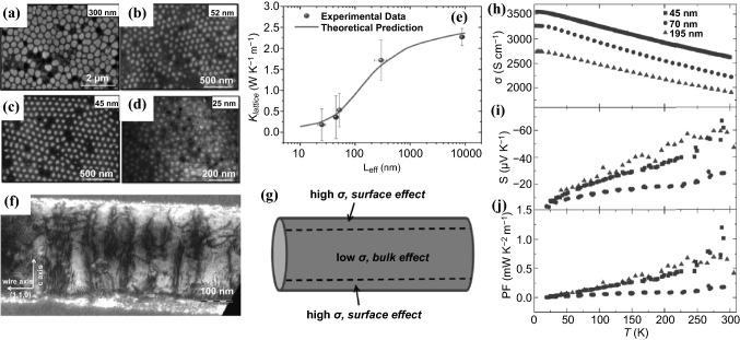
Fig. 10.
SEM images of a 300 nm, b 52 nm, c 45 nm and d 25 nm average diameter Bi2Te3 NWs. e κL of the NWs versus diameters. f TEM image of a Bi2Te3−ySey ternary NW. g Schematic of the NW showing the contribution of the surface states with a high σ, whereas bulk part yields a low electrical conductivity and a high S. Temperature-dependent h electrical conductivity, i Seebeck coefficient and j power factor of Bi2Te3−ySey ternary NWs of three different diameters (45, 70 and 195 nm). Adapted with permission from Refs. [137, 147]

