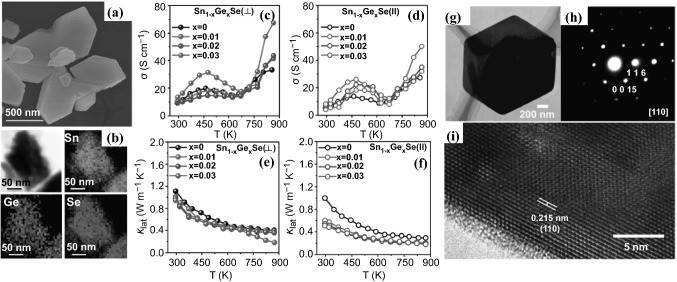
Fig. 13.
a FESEM image of Sn0.97Ge0.03Se nanoplates. b STEM image of Sn0.97Ge0.03Se nanoplates along with EDAX color mapping for Sn, Ge, and Se. Temperature-dependent c, d electrical conductivity and e, f lattice thermal conductivity of Sn1−xGexSe measured parallel (open symbols) and perpendicular (solid symbols) to the SPS pressing direction, respectively. g TEM image, h SAED pattern and i HRTEM image of a single Sb2Te3 nanoplate. Adapted with permission from Refs. [192, 193]

