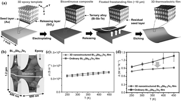
Fig. 16.
a Schematic illustration of procedures for the fabrication of a freestanding and transferrable 3D nanostructured TE film. b Structural unit cell of a 3D nanostructured Bi1.5Sb0.5Te3 film illustrating the concept of increasing phonon boundary scattering without altering electrical transport. Comparison of c electrical conductivity and d thermal conductivity of the 3D nanostructured and ordinaryBi1.5Sb0.5Te3 films as a function of temperature. Adapted with permission from Ref. [209]

