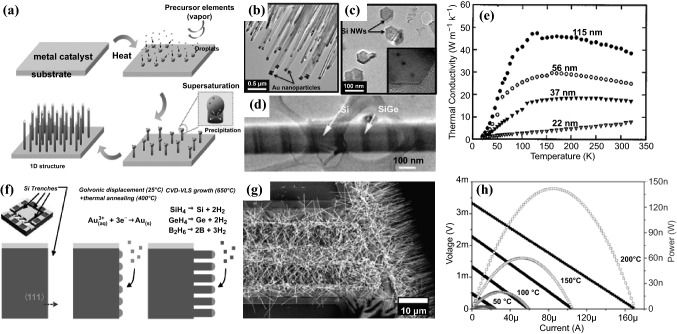
Fig. 9.
a Schematic diagram of the synthesis of the NWs by VLS growth method. b TEM image of Si NW arrays showing gold nanoparticles on the tip. c Cross-section TEM image of silicon NWs showing hexagonal shape. d TEM image of Si/SiGe superlattice NWs. e Measured thermal conductivity of different diameter Si NWs. f Schematic steps for CVD-VLS growth of boron-doped SiGe NWs and integration in μTEGs. g Top-view SEM image of SiGe NWs selectively grown in Si exposed parts. h Current–voltage and current-power curves obtained from SiGe NWs based μTEGs with three trenches for different hot plate temperatures. Adapted with permission from Refs. [127–129]

