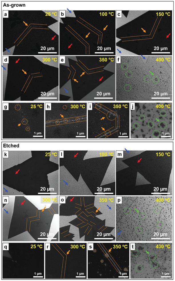
Figure 1.

SEM images of the as‐grown and etched MoS2 monolayers before (25 °C) and after annealing (100–400 °C). a–j) The SEM images of the as‐grown MoS2 monolayers a,g) before annealing (25 °C) and after annealing at b) 100 °C, c) 150 °C, d,h) 300 °C, e,i) 350 °C, and f,j) 400 °C. k–t) The SEM images of the k,q) etched MoS2 monolayers before annealing (25 °C) and after annealing at l) 100 °C, m) 150 °C, n,r) 300 °C, o,s) 350 °C, and p,t) 400 °C. The light background is the SiO2/Si wafer (blue arrow) and monolayer MoS2 appears as a dark flake (red arrow). The bright nanoparticles (enclosed by orange dotted lines and pointed by arrows) are ascribed as MoOx nanoparticles. Both the f) as‐grown and p) etched MoS2 monolayers break into small pieces (green arrow and dotted circles) after being annealed at 400 °C. Ex situ SEM images were taken from different spots in different samples.
