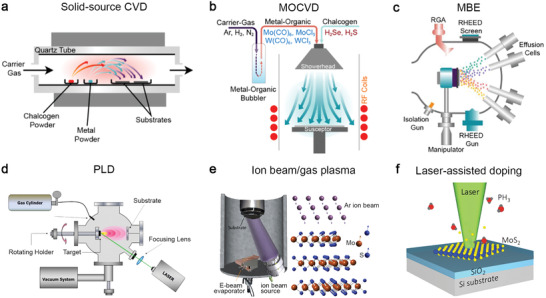
Figure 3.

Thin‐film techniques for achieving doped and alloyed 2D TMDs. a) Solid source chemical vapor deposition (CVDSS) evaporates multiple powder precursors at high temperature and deposits 2D crystals on substrates placed downstream. Reproduced with permission.[ 30 ] Copyright 2019, IOP Publishing. b) Metal‐organic chemical vapor deposition (MOCVD) uses volatile precursors delivered into the reactor by carrier gas flowing through bubbler manifolds where MO precursors are stored. Reproduced with permission.[ 30 ] Copyright 2019, IOP Publishing. c) Molecular beam epitaxy delivers multiple elemental sources at ultra‐high vacuum using the Knudsen effusion cells. RHEED and RGA are standard techniques in MBE for monitoring thickness and environmental impurity. Reproduced with permission.[ 30 ] Copyright 2019, IOP Publishing. d) Pulsed laser deposition uses plasma plumes created by laser ablation of a target using an excimer laser (e.g., 248 nm, 25 ns pulse width) to deliver stochiometric precursors to the substrate in elevated temperatures. Reproduced under the terms of CC‐BY license.[ 53 ] Copyright 2020, The Authors, published by MDPI. e) Top–down, ion beam‐ or plasma‐assisted processes convert as‐grown pristine TMD into doped/alloyed samples by generating defects and supplying dopants to fill in the defects. Reproduced with permission.[ 89 ] Copyright 2019, American Chemical Society. f) Top–down laser‐assisted chemical vapor doping of as‐grown TMDs at room temperature. The opto‐thermal energies provided by a laser can dissociate the gaseous molecules comprised of dopants and create defects on TMDs. Reproduced with permission.[ 13 ] Copyright 2016, Wiley‐VCH.
