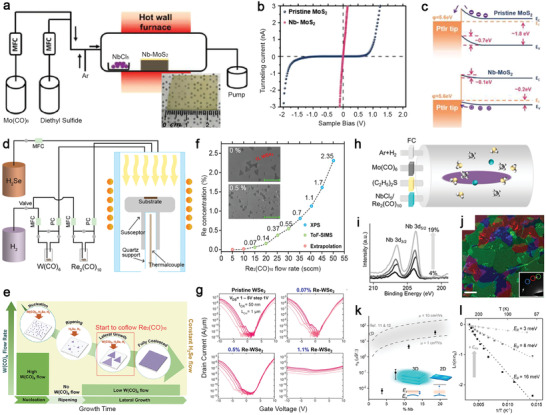
Figure 5.

Examples of doped 2D TMDs grown via the MOCVD process. a) Schematic of the hot‐wall hybrid MOCVD setup for the synthesis of Nb‐doped MoS2. A camera image of uniformly grown Nb‐doped MoS2 (NbCl5 at 55 °C) is shown in the inset. The scale bar is 1 cm. Reproduced with permission.[ 9 ] Copyright 2020, Wiley‐VCH.b) I–V characteristics of pristine MoS2 and Nb‐doped MoS2 with Nb% = 5%. The schematic of the conductive AFM measurements is shown in the inset. Reproduced with permission.[ 9 ] Copyright 2020, Wiley‐VCH.c) Schematic of type Schottky contact (top) and p‐type Ohmic contact (bottom) explains the observed diode‐Ohmic transition by Nb doping. Reproduced with permission.[ 9 ] Copyright 2020, Wiley‐VCH. d) Illustration of the vertical, cold‐wall MOCVD system that is used to grow Re‐oped WSe2 samples. Reproduced with permission.[ 96 Copyright 2020, Wiley‐VCH.e) Schematic of the multi‐step process showing variation in W(CO)6 flow rate that was used to control nucleation, ripening, and lateral growth. Re2(CO)10 flow is introduced at the lateral growth step. Reproduced with permission.[ 98 ] Copyright 2018, American Chemical Society. f) The doping data from XPS, SIMS, and extrapolated points are plotted as a function of Re2(CO)10 flow rate. Reproduced with permission.[ 96 ] Copyright 2020, Wiley‐VCH.g) Transfer characteristics of 800 °C‐grown pristine and Re‐doped WSe2 back‐gated field‐effect‐transistors on 50 nm ALD Al2O3.While ambipolar conduction in the pristine and lightly doped (0.07% and 0.5%) films is demonstrated, at higher dopant concentrations (1.1%), device performance is degraded due to the loss of semiconducting nature. Reproduced with permission.[ 96 ] Copyright 2020, Wiley‐VCH. h) Schematic of the MOCVD system for the growth of doped MoS2 using gas‐phase precursors. Metering valves are used as the flow controllers for the Nb and Re precursors, while MFCs are used for the other precursors and carrier gases. Reproduced with permission.[ 97 ] Copyright 2020, American Chemical Society. i) XPS spectra show doping concentrations for different Nb‐MoS2 samples. From bottom to top: C Nb = 4%, 8%, 11%, and 19%. Reproduced with permission.[ 97 ] Copyright 2020, American Chemical Society. j) ADF‐TEM image of Nb‐doped MoS2 shows misoriented domains in false colors with the corresponding diffraction pattern shown in the inset. The scale bar is 200 nm. Reproduced with permission.[ 97 ] Copyright 2020, American Chemical Society.k) Semi‐log plot of average σ S versus C Nb. The dash lines represent the theoretical σ S assuming full ionization, with mobilities taken to be 10 and 1 cm2 (V−1 s−1) for upper and lower dash lines, respectively. Inset: Band diagram shows the dopant carriers in 2D materials cannot be thermally activated at room temperature due to high activation energy (kT shown in light orange). The glow around the cyan circle indicates the a0. E V represents the valence band, and E I represents the dopant energy level. Reproduced with permission.[ 97 ] Copyright 2020, American Chemical Society.l) Arrhenius plot of devices with C Nb = 8%, 11%, and 19% (from bottom to top, respectively). The best fit line for each data set is used to extract E 0. The electrical conductance at various temperatures is normalized to the room‐temperature conductance (σ R). Reproduced with permission.[ 97 ] Copyright 2020, American Chemical Society.
