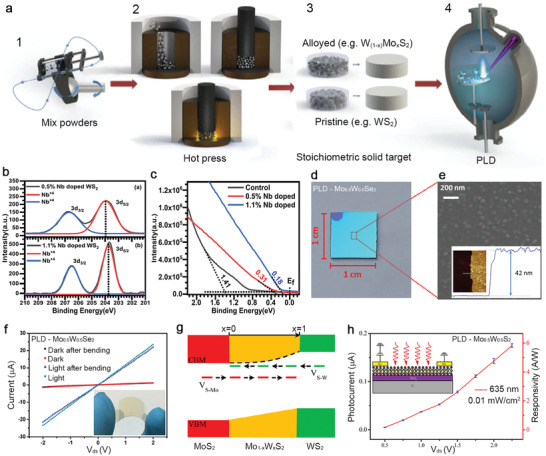
Figure 7.

Pulsed laser deposition for doped and alloyed TMDs. a) Illustration of ablation target fabrication and process flow consists of: 1) mixing pristine TMD powders and powders of interest for doping and alloying; 2) hot pressing uniformly mixed powders at elevated temperatures to form; 3) stoichiometric targets for laser ablation; and 4) synthesis of alloyed TMDs films in PLD. Reproduced with permission.[ 105 ] Copyright 2016, American Chemical Society. b) Nb 3d XPS spectra of the 0.5 and 1.1 atomic percentage (at%) Nb‐doped WS2 films grown by PLD. Reproduced with permission.[ 106 ] Copyright 2018, AIP Publishing. c) Valence band edge of undoped WS2, and 0.5 and 1.1 at% Nb‐doped WS2 film with respect to Fermi level indicates the Fermi level shifts toward the valance band edge with the increased Nb incorporation. Reproduced with permission.[ 106 ] Copyright 2018, AIP Publishing. d) Camera image of a PLD‐grown Mo0.5W0.5Se2 alloy film on 1 cm2 SiO2/Si. The top left corner of the substrate provides the contrast of bare silica. Reproduced with permission.[ 107 ] Copyright 2017, American Chemical Society. e) The scanning electron micrograph of an as‐grown Mo0.5W0.5Se2 film provides a close view of compact nanodomains on the surface. The inset shows the thickness of the same film. Reproduced with permission.[ 107 ] Copyright 2017, American Chemical Society. f) I−V characteristics of the flexible two‐terminal device are acquired in the dark and under light illumination. Inset shows a camera image of a flexible Mo0.5W0.5Se2 alloy film under bending deposited on a PI substrate. Reproduced with permission.[ 107 ] Copyright 2017, American Chemical Society. g) Illustration of the energy band diagram for Mo 1− xWxS2 alloys as a function of x. Reproduced with permission.[ 108 ] Copyright 2016, American Chemical Society.h) Voltage‐dependent photocurrent and responsivity of the Mo 1− xWxS2 detector under the illumination of a 635 nm laser. Inset is a schematic of the photodetector. Reproduced with permission.[ 108 ] Copyright 2016, American Chemical Society.
