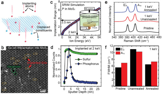
Figure 9.

Ion implantation for doping 2D TMDs. a) Schematic of energetic implanting dopants (red) that sputter of the constituents of 2D materials and fill in the vacancies to complete substitutional doping. Reproduced with permission.[ 125 ] Copyright 2013, American Chemical Society. b) Gaussian‐filtered ADF‐STEM image of Se ions‐implanted MoS2 monolayer. Orange and green rings are SSe pairs and vacancies created by Se implantation. Reproduced with permission.[ 79 ] Copyright 2016, Elsevier. c) SRIM simulation data shows the implantation range of P in MoS2 for increasing ion energy in the PIII process. d) SIMS profiles obtained from P‐implanted MoS2 show shallow phosphorus doping with a sharp Gaussian‐like distribution compared to background S. e) Raman spectra and f) FWHM values of Raman peaks (E 1 2g and A 1g) for pristine, implanted by P at 1 keV (unannealed), and post‐implantation annealed MoS2. (c‐f): Reproduced with permission.[ 12 ] Copyright 2016, American Chemical Society.
