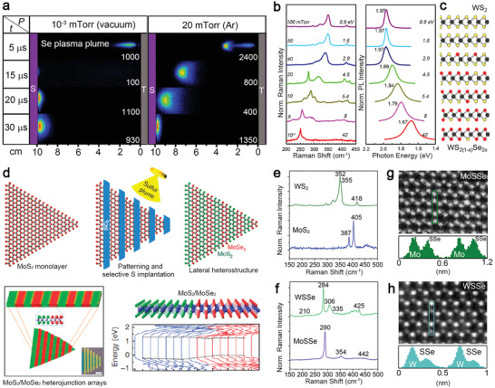
Figure 10.

Hyperthermal energy implantation for doping 2D materials by PLD. a) False color, gated‐ICCD images of the Se plasma plume's visible luminescence reveal the plume's propagation dynamics through the vacuum and 20 mTorr Ar background gas pressures at the indicated delay times following the laser pulse. (Gate width is 10% of each delay time. The maximum intensity is shown for comparison.) b) Raman spectra of WS2 monolayers on SiO2/Si substrates (left) and their corresponding PL spectra and peak energy positions (right) exposed by 800 Se plasma plume pulses in different Ar background gas pressures and plume kinetic energies at 250 °C. Spectra indicate an increasing fraction of Se incorporation in WS2(1− x )Se2 x with decreasing Ar pressure. c) Schematic structural evolution of Se incorporation in WS2(1− x )Se2 x corresponding to the Raman/PL spectra in (b). (a‐c): Reproduced with permission.[ 67 ] Copyright 2020, American Chemical Society. d) Schematic for the formation of lateral MoSe2/MoS2 heterojunction arrays within a monolayer by patterning with SiO2 hard masks and selective conversion using S plasma plume (top row). Green, red, and combined Raman maps were obtained from corresponding optical images representing MoS2 and MoSe2 at 403 and 238 cm−1. Scale bar is 5 µm. First‐principles calculations of a lateral MoSe2/MoS2 junction show formation of type‐I band alignment. Reproduced under the terms of the CC‐BY 4.0 license.[ 126 ] Copyright 2015, The Authors, published by Springer Nature. e) Raman spectra of as‐grown CVD MoS2 and WS2 monolayers. f) Raman spectra of the Janus MoSSe and WSSe monolayers converted from the same samples are shown in (e). g,h) ADF‐STEM image of MoSSe (g) and WSSe (h) and the Z‐contrast intensity profiles in the highlighted sections in the images verify the Janus structure. (e‐h): Reproduced with permission.[ 67 ] Copyright 2020, American Chemical Society.
