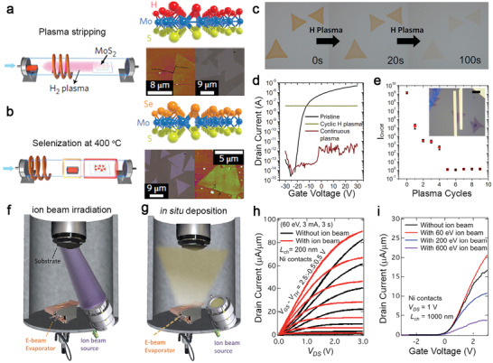
Figure 11.

Modifying compositions and structures in 2D semiconductors through vacancies. a) A MoS2 monolayer was exposed to H2 plasma to strip the top‐layer S. The plasma was then switched off, and Se powder loaded in a quartz boat was moved next to the sample without breaking the vacuum. b) Se was then thermally vaporized to achieve selenization and complete the synthesis of Janus MoSSe. Optical micrograph and AFM images for each structure are shown below the molecular model for each stage. (a‐b): Reproduced with permission.[ 88 ] Copyright 2020, AIP Publishing. c) Optical micrographs of pristine MoS2 and after various H2 plasma exposure time. d) Transfer curves for pristine and cyclic and continuous H2 plasma exposed MoS2. e) On/off ratio as a function of the cycles of “10 s plasma + atmosphere exposure”. An optical micrograph of the tested FETs is shown in the inset. The scale bar is 5 µm. (c‐e): Reproduced under the terms of CC‐BY 4.0 license.[ 129 ] Copyright 2019, The Authors, published by Springer Nature. f) Experimental setup of the in situ convergent Ar+ ion beam source with an e‐beam evaporator within an ultra‐high vacuum (UHV) chamber. The ion beam irradiation first creates defects in samples. g) In situ Ni evaporation process was carried out right after ion beam exposure. (f‐g): Reproduced with permission.[ 89 ] Copyright 2019, American Chemical Society. h) Comparison of the output characteristics of the FET fabricated on both irradiated and pristine MoS2 with Ni contact. i) Comparison of the effect of different ion beam energies on device transfer characteristics. The ion beam exposure conditions are (60 eV, 3 mA, 3 s), (200 eV, 3 mA, 3 s), and (600 eV, 36 mA, 3 s), respectively. (h‐i): Reproduced with permission.[ 136 ] Copyright 2020, Royal Society of Chemistry.
