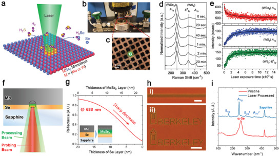
Figure 12.

Laser‐assisted modifications and growth of TMD crystals. a) A schematic of the laser‐assisted S‐Se conversion in an H2S atmosphere. b) Image of the mini environmental chamber under the microscope‐based laser spectrometer. c) The laser beam (green) focused on a WSe2 monolayer suspended on a TEM grid. d) Time‐dependent evolution of the Raman spectra for the WSe2 (A 1g) and WS2 (A 1g and E 2g) under laser irradiation (532 nm, 0.7 mW) in an H2S atmosphere. e) Time‐dependent evolution of the Raman peak intensity. (a‐e): Reproduced with permission.[ 82 ] Copyright 2018, Wiley‐VCH. f) A schematic of the laser‐assisted growth ofMoSe2 from the sapphire/Se/Mo multilayer stack. In situ reflectance measurement showing the processing time for the saturation of MoSe2 growth. g) Calculated reflectance of the Se/MoSe2/Mo multilayer at a 633 nm laser beam incident from the sapphire side as a function of the Se layer's thicknesses and the MoSe2 layer formed. The laser beam was irradiated through the transparent sapphire substrate, and MoSe2 was formed at Se/Mo interface (inset). h) Optical micrographs obtained through the sapphire substrate show laser‐written (i) simple line and (ii) arbitrary patterns. The scale bars in panels (i) and (ii) are 10 and 100 µm, respectively. (i) Raman spectra obtained from the pristine and laser‐processed area. (f‐i): Reproduced with permission.[ 84 ] Copyright 2020, American Chemical Society.
