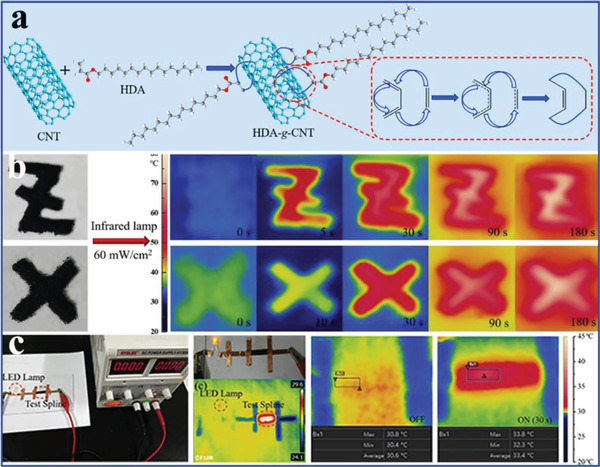
Figure 11.

a) Preparation scheme of HDA‐g‐SWCNTs and HDA‐g‐MWCNTs. b) FLIR camera images of HDA‐g‐MWCNTs, and HDA‐g‐SWCNTs. c) Digital photos of the electrical conductivity experimental design and FLIR camera images of HDA‐g‐SWCNT film under 30 V. Reproduced with permission.[ 79 ] Copyright 2019, Elsevier.
