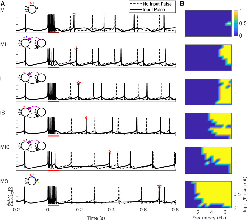
Fig 7. Delay of spiking in response to single pulse determines phase-locking to slow inputs.
(A) Voltage traces are plotted for simulations both with (solid lines) and without (dotted lines) an input pulse lasting 50 ms. Red bar indicates the timing of the input pulse; red star indicates the first post-input spike. (B) The phase-locking value is estimated from the response to a single input pulse using Eq (1). Frequency was calculated as 1/(4*(pulse duration)), where pulse duration is in seconds. Input per pulse was calculated by integrating pulse magnitude. The magenta line indicates 7 Hz.

