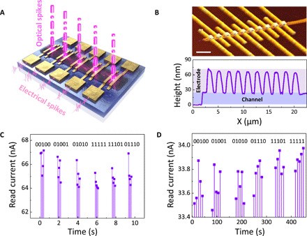
Fig. 2. Dynamic memristor circuit and corresponding responses to optical and electrical stimuli.

(A) Schematic of a multifunctional memristor array stimulated by various electrical and optical inputs. (B) An AFM image and line profile of a device array used in this study. Scale bar, 2 μm. (C) Experimental read-current responses of a memristor by several electrical input signals, (00100), (01001), (01010), (11101), (01110), and (11111). The amplitude and width of the read pulses are correspondingly 1 V and 25 ms. (D) Experimental read-current responses of a memristor by several optical input signals (725 nm and 42 mW) with corresponding width and intervals of 5 and 3 s. The read voltage for the optical pulses was 0.5 V.
