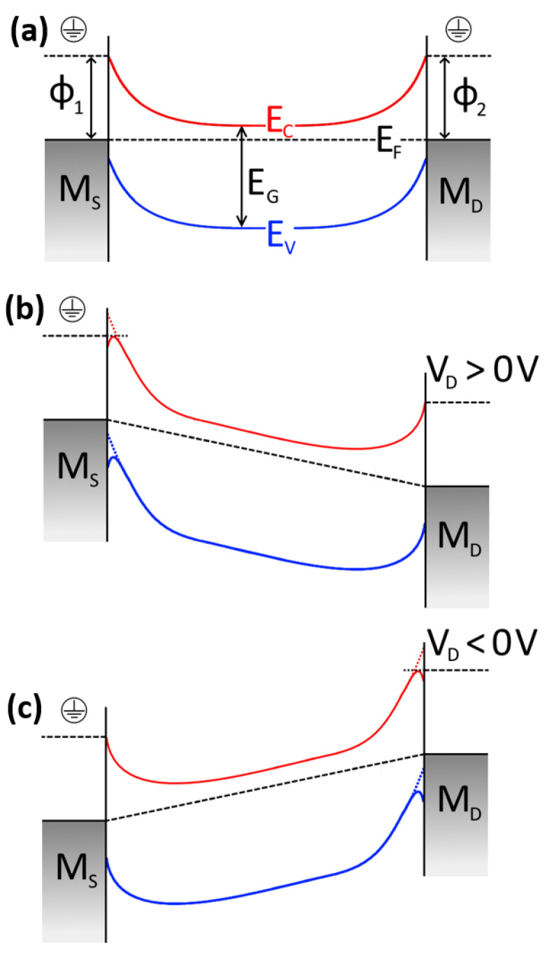
Figure 4.
Metal-Semiconductor-Metal band diagram for: (a) both Schottky junctions at ground potential, (b) MS (source metal) in ground potential and MD (drain metal) with a positive voltage applied, and (c) MS in ground potential and MD with a negative voltage applied. EC, EV, EF, and EG represent the conduction band, valence band, Fermi level band, and the semiconductor bandgap, respectively.

