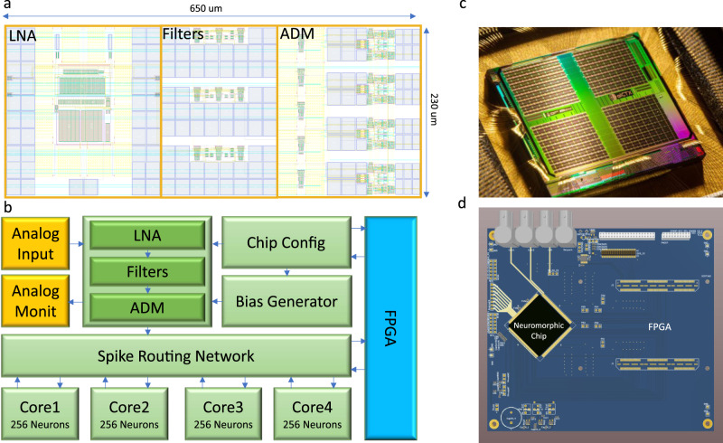
Fig. 2. Neuromorphic electronic system overview.
a Physical layout of a single channel of the analog headstage array, including the LNA, three low-pass/band-pass filters, and four ADM signal to spike encoders. b Reduced block diagram of the neuromorphic platform. Analog signals from electrodes are fed into the input headstage that converts them into spike trains and sends them to the SNN implemented on the multi-neuron cores, via a spike routing network. The spike routing network routes the spikes within on-chip SNN and to an external FPGA device used for data logging and prototyping. The FPGA is also used for setting circuit parameters. c Chip photograph showing the 11 mm x 9 mm silicon die. d Prototyping Printed Circuit Board (PCB) used to host the chip and the infrastructure to implement the test setup. The setup is composed of a prototyping FPGA board mounted on the same PCB that hosts the chip, and of probe points to evaluate the characteristics of both input headstage and SNN multi-core network.

