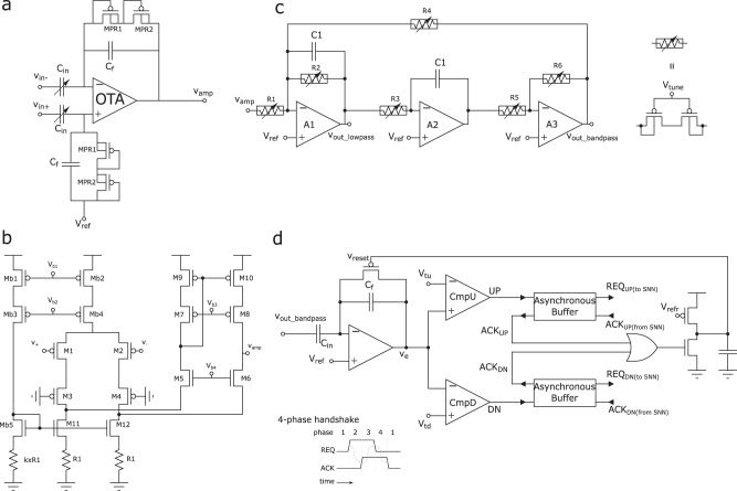
Fig. 3. Schematic diagrams of the input headstage circuits.
a Variable-gain LNA using variable input capacitor array and pseudo-resistors. The gain of this stage is calculated by Cin/Cf; the use of the pseudo-resistors allows to reach small low cut-off frequencies. b Folded cascode OTA using resistive degeneration to reduce the noise influence of nMOS devices. Note that the current flowing through the biasing branch, Mb1-Mb3-Mb5-k × R1, is k times smaller than the tail branch of the amplifier. c band-pass (Tow-Thomas) filters for performing second-order filtering in both ripple and fast-ripple bands as well as the low-frequency component of the iEEG. Tunable pseudo resistors are used to adjust the filter gain, center-frequency, and band-width. The same basic structure can be used to provide both low-pass and band-pass outputs, thus is desirable in terms of design flexibility. d Asynchronous Delta Modulator (ADM) circuit to convert the analog filter outputs into spike trains. The ADM input amplifier has a gain of Cin/Cf in normal operation when Vreset is low and the feedback PMOS switch is off. As the amplified signal crosses one of the two thresholds, Vtu or Vtd, a UP or DN spike is produced by asserting the corresponding REQ signal. A 4-phase handshaking mechanism produces the corresponding ACK signal in response to the spike. Upon receiving the ACK signal, the ADM resets the amplifier input and goes back to normal operation after a refractory period determined by the value of Vrefr. The asynchronous buffers act as 4-phase handshaking interfaces that propagate the UP/DN signals to the on-chip AER spike routing network of Fig. 2.

