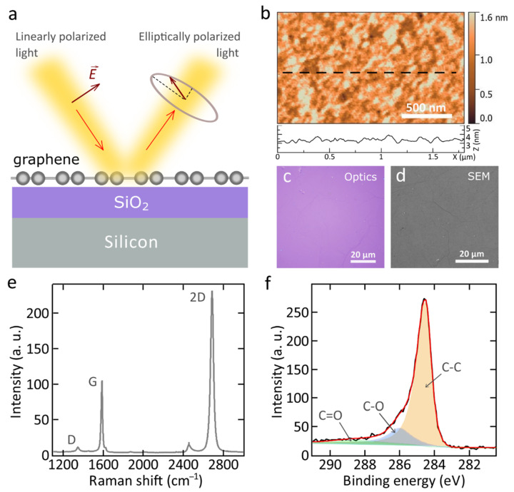
Figure 1.
(a) The scheme of the ellipsometry measurements. (b) AFM topography mapping of single-layer graphene on SiO2/Si substrate with line profile across the surface. The scan area was 1.8 × 1.1 μm2. (c) Optical image of the graphene on top of SiO2/Si substrate. (d) SEM image of the graphene reveals a high crystallinity of the samples with the crystallite size larger than 10 μm. (e) Raman spectrum of graphene transferred on SiO2/Si substrate, at excitation wavelength λ = 532 nm. (f) Results of XPS fitting analysis of the C1s core level signal obtained for the monolayer graphene on SiO2/Si.

