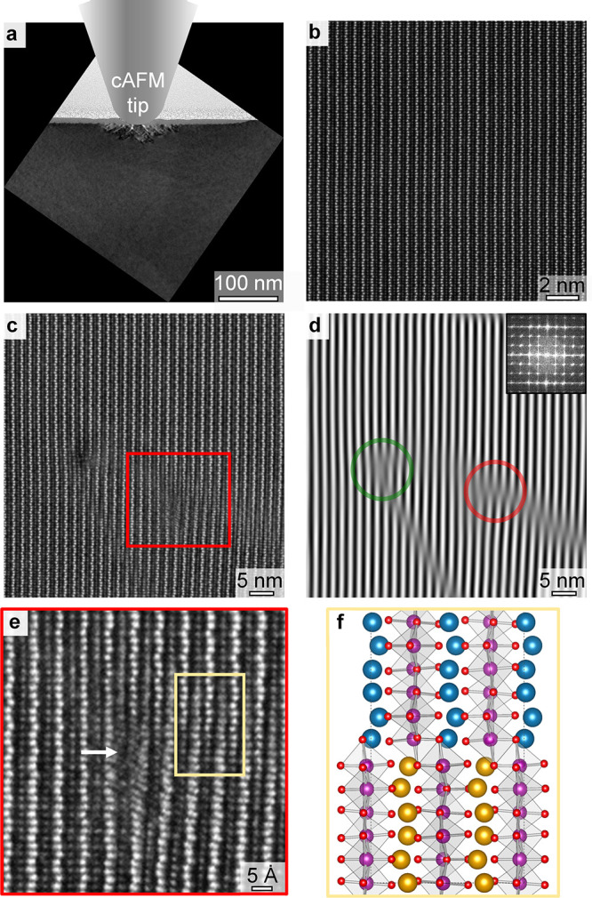
Figure 2.

Atomic-scale structure of electrically induced dislocations and stacking faults. (a) Bright-field TEM image and schematic of the cAFM tip, illustrating that the perturbed crystal structure is restricted to the area beneath the cAFM tip. (b) HAADF-STEM image viewed down the [1̅00] direction, showing the as-grown state. (c) HAADF-STEM image viewed down the [1̅00] direction, showing the region beneath the position of the AFM tip after the application of the electric field. The periodic crystal structure is interrupted by line features extending in directions close to the ⟨011⟩ directions. The bright and gray dots are Er and Mn atomic columns, respectively. (d) Inverse fast Fourier transformation (FFT) obtained by selecting only the (002) maxima of an FFT of panel b; see the insert. The image shows areas with the same periodicity of the Er lattice, allowing easier identification of lattice defects. Two edge dislocations are highlighted by red and green circles. (e) Representative HAADF-STEM image taken across the crystallographic features, corresponding to the area marked by the red box in panel c. (f) Fully relaxed DFT supercell, modeling the dislocated structure by unit cells dislocated by c/4 and a/3 with respect to each other. Large gold and blue spheres represent Er atoms on either side of the stacking fault; Mn and O atoms are sketched in purple and red, respectively.
