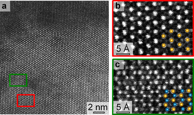
Figure 3.

Atomic defect structure viewed along the [001] axis. (a) HAADF-STEM image of a region with electric-field induced defects, written with the same parameters as used in Figures 1 and 2. Bright dots correspond to Er atom columns. (b) HAADF-STEM image of the area represented by the red box of panel a, showing the expected Er cation lattice for a hexagonal crystal when viewed along the [001] direction. The gold dots correspond to a DFT simulation of the structure, looking down the [001] axis. Mn columns can be seen as weak dots in between the more pronounced dots from the Er columns. (c) HAADF-STEM image corresponding to the area represented by the green box in panel a, showing the Er pattern that deviates from the unperturbed crystallographic structure seen in panel b. Gold and blue dots represent the bulk and shifted Er atom columns when the stable dislocation of Figure 2 is viewed down the [001] axis. The overlay shows that the dislocated structure reproduces the pattern resolved by HAADF-STEM.
