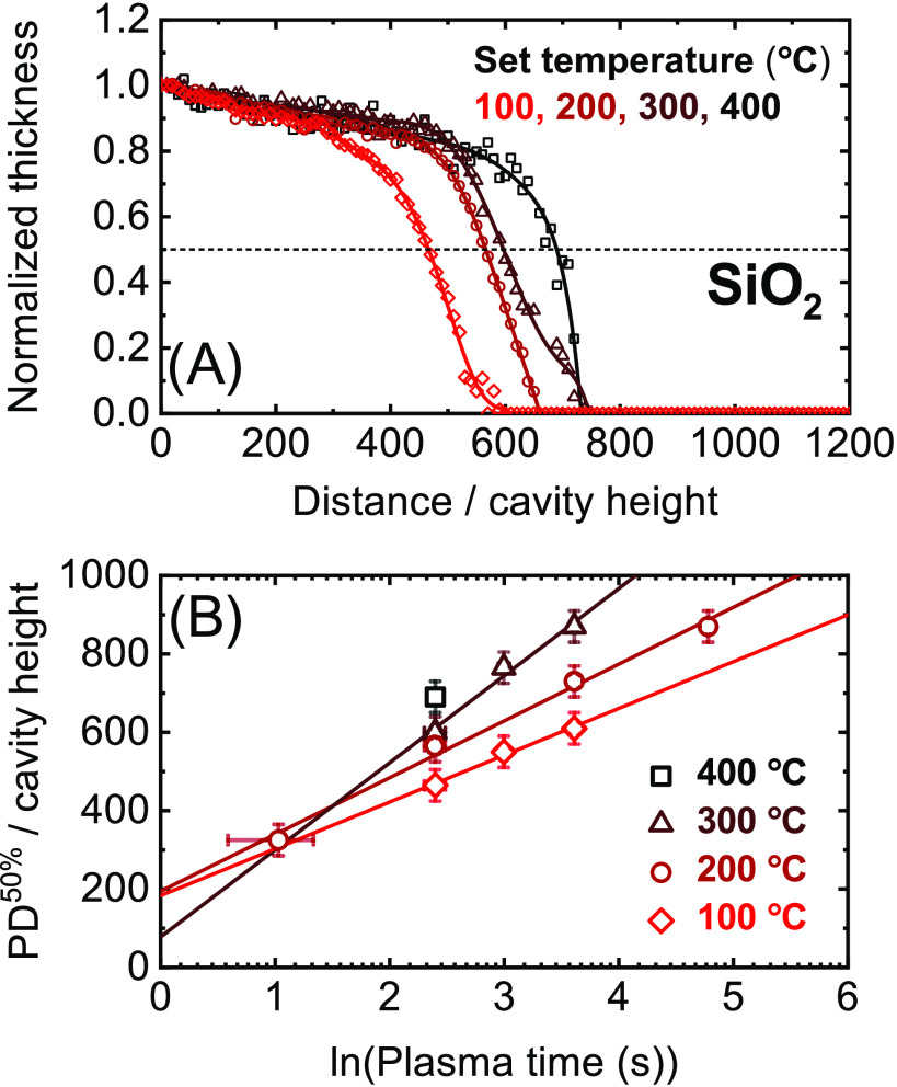
Figure 2.
Panel (A): Normalized thickness profiles of SiO2 films grown by plasma ALD on lateral-high-aspect-ratio (LHAR) cavity structures at different temperature setpoints and a fixed plasma exposure time of 12 s per ALD cycle. Similar thickness profiles have been determined for plasma exposure times other than 12 s (at 100, 200, and 300 °C, see the Supporting Information), of which the scaled half-thickness penetration depths are plotted in panel (B).

