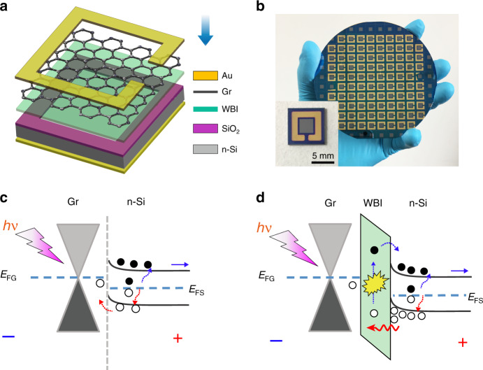
Fig. 1. Device structure and proposed working mechanism for the devices.
a Schematic and b photo image of the fabricated wafer-scale graphene/insulator/Si (GIS) heterojunction photodetectors. The device size was 8 × 8 mm2 with a center active region of 3 × 3 mm2. c, d Shows the corresponding energy band diagram of the conventional GS heterojunction photodetector and the GIS heterojunction photodetector under reverse bias and illumination, respectively.

