
Fig. 1. Schematics of a dielectric–graphene–dielectric–metal (GDM) heterostructure.
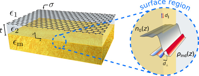
The graphene–metal separation, t, is controlled by the thickness of the dielectric (ϵ2) spacer. The close-up (near the metal–spacer interface) shows a pictorial representation of the surface–response functions d⊥ and d∥ along with the related the microscopic quantities characterizing the metal surface, namely the equilibrium electronic density, n0(z), and the induced charge density, ρind(z).