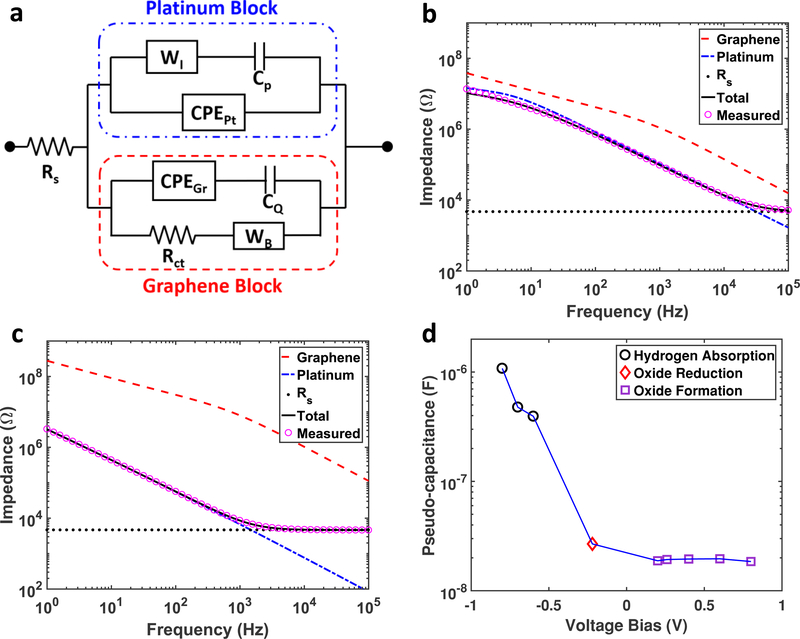
Figure 4.
(a) Equivalent circuit model contains two blocks for graphene and PtNPs respectively. The parameters for the graphene block are fixed according to Table 1 and the coverage percentage according to SEM images. The PtNPs block and solution resistance (Rs) is obtained by fitting the measurement data to the circuit model. WI, Cp, and CPEPt are the infinite Warburg element, pseudo-capacitance, and constant phase element for Pt double layer capacitor respectively. (b) Impedance of the graphene block (red dashed curve), Pt block (blue dashed curve) with respect to the total impedance of measurement (pink hollow circles) and fitting (black curve). The PtNPs block dominates the impedance over the graphene block at all frequencies. (c) This effect is more obvious for 50 seconds deposition, except at frequencies above 40 KHz, where solution resistance starts to dominate. (d) The fitted pseudo-capacitance of 50 seconds deposition with respect to the voltage bias shows at the pseudo-capacitance increases as the bias approaches hydrogen absorption region.

