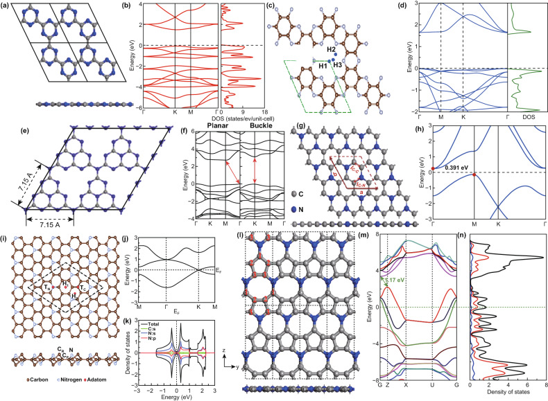
Fig. 4.
a Top view and side view of the supercell (2 × 2) g-C3N3. b Band structure and total density of state for 1 × 1 g-C3N3. Reproduced with permission from Ref. [15]. c Relaxed structure of 2 × 2 C2N monolayer, H1, H2, and H3 are possible binding sites for transition metal atom doping on the C2N. d Band structure and density of states of C2N monolayer. Reproduced with permission from Ref. [28]. e Schematic structure of monolayer g-C3N4. Reproduced with permission from Ref. [18]. f Calculated band structures of monolayer g-C3N4 with planar or buckled topology. Reproduced with permission from Ref. [20]. g Optimized structure and h band structure of C3N monolayer. The unit cell is shown by the red dashed line. Reproduced with permission from Ref. [29]. i Top and side view of the atomic structure of monolayer C4N. The black dashed lines show the 3 × 3 × 1 supercell of monolayer C4N. Four adsorption sites were considered (H1, H2, TC, TN). j Electronic band structures and k PDOS of the unit cell of a pristine C4N monolayer. Reproduced with permission from Ref. [30]. l Top (upper) and side (lower) view of the atomic structure of C5N monolayer. The gray and blue balls represent C atoms and N atoms, respectively. m Band structure and n density of states (DOS) of C5N monolayer obtained from HSE06 calculations. The black, red, and blue lines denote the total DOS of C5N, the partial DOS of C atoms, and the partial DOS of N atoms, respectively. Reproduced with permission from Ref. [27]. Copyright permissions from Elsevier, Royal Society of Chemistry and Wiley–VCH. (Color figure online)

