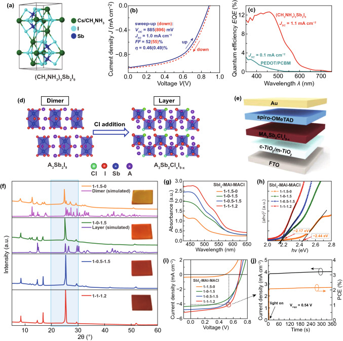
Fig. 14.
a Crystal structure of (CH3NH3)3Sb2I9 (space group P63/mmc). b Illuminated J–V curves of (CH3NH3)3Sb2I9 solar cell measured with forward and backward scanning with a rate of 0.1 V s−1. c EQE measurement of the (CH3NH3)3Sb2I9 solar cell compared to the reference device of ITO/PEDOT/PCBM/ZnO-NP/Al. Reproduced with permission from Ref. [173] d Schematic plot of the Cl doping-induced transformation from the 0D dimer phase of A3Sb2I9 to the 2D layered phase of A3Sb2ClXI9−X. e Schematic structure of the as-fabricated PSC. f XRD patterns of the films deposited from precursors containing SbI3, MAI, and MACl with molar ratios of 1:1.5:0, 1:0:1.5, 1:0.5:1.5, and 1:1:1.2. g Measured UV–vis absorbance spectra of the four types of films. h Tauc plots of the absorption coefficients for evaluating the bandgap values of the pure-iodine perovskites MA3Sb2I9 and Cl-containing mixed-halide perovskites MA3Sb2ClXI9−X. i J–V curves for the devices fabricated with the four kinds of perovskite films. j Steady-state photocurrent output for the device based on 1-1-1.2 film at the maximum power point (red circle). Maximum power point voltage Vmpp is equal to 0.54 V. Reproduced with permission from Ref. [176]

