
Figure 6.
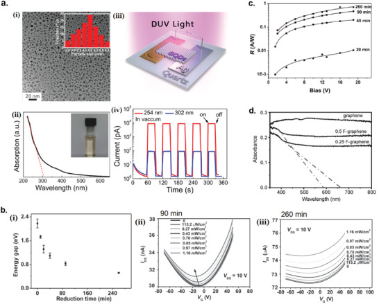
Bandgap engineering of graphene‐based photodetectors. a) GQD deep‐UV photodetector. i) TEM image of the GQDs. Inset: size distribution of the GQDs. ii) UV–vis absorption spectrum of the GQDs. Inset: photo of the aqueous solution of the GQDs. iii) Schematic of the GQD photodetector with asymmetric electrode configuration. iv) Photoresponse transients of the device under pulsed 254 and 302 nm DUV light (42 µW cm−2). The voltage bias was 5 V. Reproduced with permission.[ 130 ] Copyright 2015, American Chemical Society. b) Controlling the bandgap of rGO by thermal reduction. i) The bandgap of rGO as a function of reduction time. ii) I DS–V G curves of rGO FET thermally reduced for 90 min under irradiation at 370 nm. iii) I DS–V G curves of rGO FET thermally reduced for 260 min under irradiation at 370 nm. Reproduced with permission.[ 80 ] Copyright 2010, WILEY‐VCH. c) Responsivity as a function of bias for rGO/SiO2/Si‐based infrared photodetector based with different reduction times of rGO (0, 20, 40, 90, 260 min). Incident radiation power is ≈14 mW cm−2. Reproduced with permission.[ 79 ] Copyright 2013, American Chemical Society. d) Diffuse reflectance spectroscopy of the as‐made graphene, 0.25 F‐graphene, and 0.5 F‐graphene. Reproduced with permission.[ 136 ] Copyright 2011, WILEY‐VCH.