Figure 13.

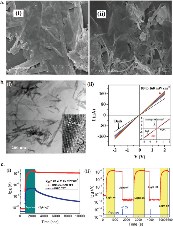
Graphene/semiconductor hybrid photodetectors. a) rGO/HfX3(X = Se and S) hybrid photodetectors. SEM images of i) rGO/HfSe3 composites and ii) rGO/HfS3 composites. Reproduced with permission.[ 106 ] Copyright 2017, Elsevier Ltd. b) rGO/Cd1‐ xZnxS hybrid photodetector. i) TEM image of the rGO/CdZnS composite. Inset: the HRTEM image of the composite. ii) I–V characteristics of rGO/CdZnS hybrid photodetector. Reproduced with permission.[ 108 ] Copyright 2017, Springer Nature. c) FLG/IGZO hybrid photodetector. i) Photocurrent transient of a‐IGZO and FLG/a‐IGZO photodetector with zero gate bias and under a light pulse (50 mW cm−2). ii) Cycling responses of the optical programming and electrical erasing of the FLg/a‐IGZO photodetector. A short positive gate‐voltage pulse (+15 V, 600 ms) was applied at 1620 and 3910 s to erase the memory effect. Reproduced with permission.[ 137 ] Copyright 2015, American Chemical Society.
