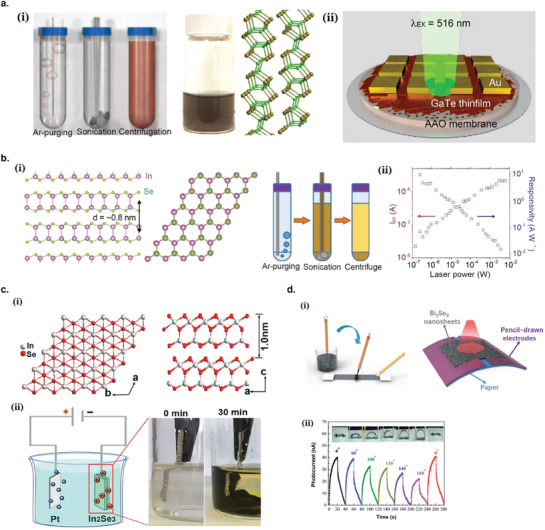
Figure 24.

Photodetectors based on layered III–VI semiconductors and topological insulators. a) GaTe photodetector. i) Schematic of the GaTe nanosheet dispersion preparation steps that minimize exposure to ambient air during processing and the atomic structure of layered GaTe (Ga: green, Te: brown). ii) Schematic of an array of percolating GaTe nanosheet thin film photodetectors. Reproduced with permission.[ 164 ] Copyright 2018, American Chemical Society. b) InSe photodetector. i) Schematic of the layered InSe crystal structure and the schematic of the preparation process for InSe dispersions using deoxygenated ethanol/water mixture. ii) Power dependence of photocurrent I pc (red) and responsivity (blue) of InSe photodetector. Reproduced with permission.[ 165 ] Copyright 2018, WILEY‐VCH. c) In2Se3 photodetector. i) The atomic structure of layered In2Se3 crystal. ii) Schematic illustration of the electrochemical exfoliation of bulk In2Se3. Reproduced with permission.[ 167 ] Copyright 2020, WILEY‐VCH. d) Bi2Se3 photodetector fabricated via pencil drawing method. i) Schematic diagram of the device fabrication process using a pencil and Chinese brush on paper. ii) Photocurrent transients of the fexible photodetector under different bending angles. Reproduced with permission.[ 168 ] Copyright 2020, Royal Society of Chemistry.
