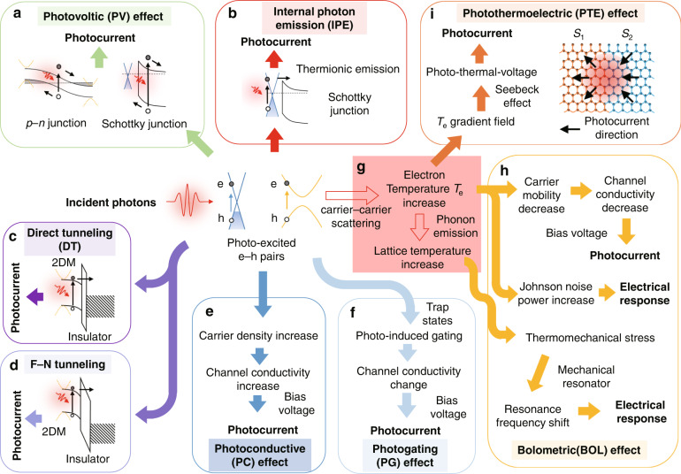
Fig. 1. Summary of the working mechanisms of 2DM PDs.
a–f Photon-type mechanisms: a The photovoltaic (PV) effect. The photo-excited e-h pairs driven by the built-in electric fields contribute to the photocurrents. b The internal photon emission (IPE) effect. For example, in a G-Si Schottky junction, the photo-excited hot carriers in graphene emitted over the Schottky barrier contribute to the photocurrent. c The direct tunneling (DT). d The Fowler-Nordheim (F-N) tunneling. e The photoconductive (PC) effect. The carrier density increment leads to the change of channel conductivity in a phototransistor. f The photo-gating (PG) effect. The photo-induced gating leads to the change of the channel conductivity in a phototransistor. g The thermal relaxation process in 2DMs. The carrier–carrier scattering results in the increment of the electron temperature Te, and then the optical/acoustic phonon emissions lead to the increment of lattice temperature TL. h, i Thermal-type mechanisms: h The bolometric (BOL) effect. The increment of Te or TL can be extracted by different read-outs. i The photo-thermoelectric (PTE) effect. Here Seebeck effect plays a major role. In the present example, S1 and S2 are respectively the positive and negative Seebeck coefficients.

