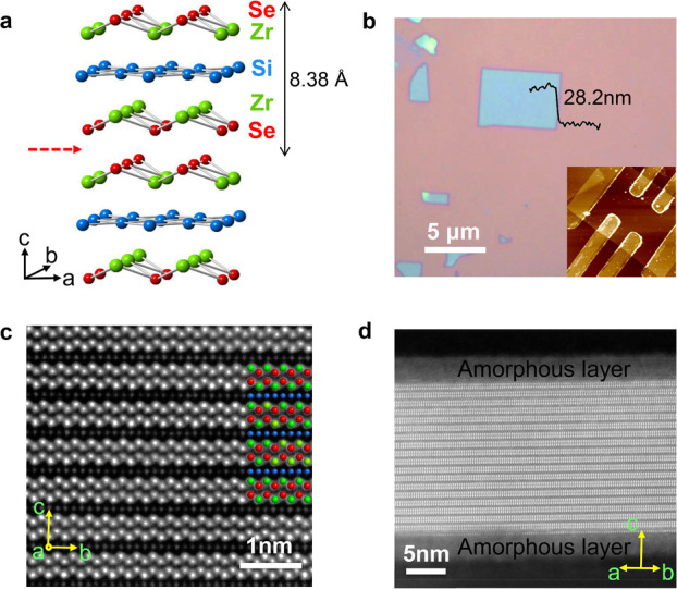
Figure 1.

ZrSiSe crystal structure and microscopy characterizations. (a) Crystal structure of ZrSiSe, showing the Se–Zr–Si–Zr-Se slabs and the cleavage plane (red arrow). (b) Optical microscope image of a 28.2 nm ZrSiSe nanoflake on Si/SiO2 wafer obtained through micromechanical exfoliation. Inset, atomic force microscope image of a Hall bar device. (c, d) Atomic resolution annular dark-field (ADF) aberration-corrected scanning transmission electron microscopy (STEM) images of (c) the bulk along the [100] zone and (d) exfoliated ZrSiSe flakes along the [110] zone. Inset in c, the [100] zone (cross-section) image matches well with the crystal structure.
