Figure 6.
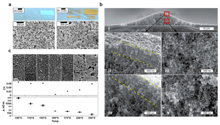
Metal nanoparticles for printed electronics. (a) photos and SEM images of inkjet-printed films with Ag (left) and Au (right) NPs. (reprinted under Creative Commons license CC BY 4.0 from Adv. Radio Sci. (2019), 17:119–127.) (b) SEM images of an AgNP deposition cross-section, showing the overall structure (i), surface (ii and iv) and interior (iii and v) after rapid laser sintering. (reprinted with permission from Appl. Sci. (2020), 10(1), 246. Copyright 2019, MDPI). (c) SEM images of AgNP films sintered at various temperatures, with corresponding graphs depicting the coefficient of variance and resistivity (reprinted with permission from Materials (2011), 4(6), 963–979, Copyright 2011, MDPI).

