Figure 7.
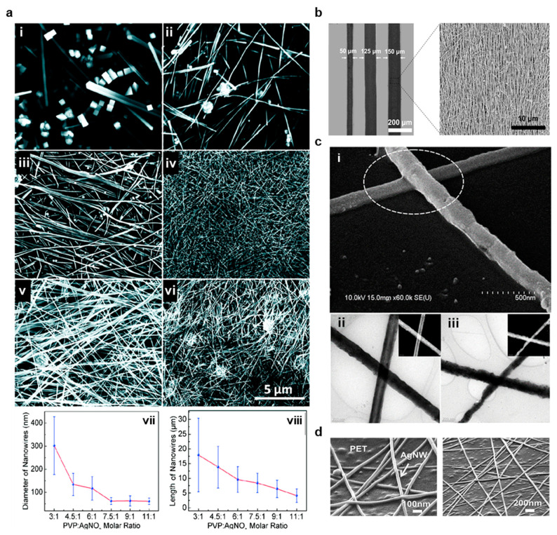
Metal nanowire synthesis, printing, and welding. (a) SEM images of Ag nanowires synthesized at different PVP:AgNO3 molar ratios of (i) 3:1, (ii) 4.5:1, (iii) 6:1, (iv) 7.5:1, (v) 9:1, and (vi) 11:1. All scales are the same. Changes in (vii) nanowire diameter and (viii) length with PVP:AgNO3 molar ratio are also shown. (reprinted with permission from Cryst. Growth Des. (2011), 11, 11, 4963–4969, Copyright 2011, ACS). (b) Images of gravure printed AgNW traces with various thicknesses and an SEM image demonstrating the aligned AgNW network. (reprinted with permission from Sci. Rep. (2018), 8, 15167, Copyright 2018, Nature Publishing Group). (c) SEM image of CuNWs nanowelded with laser irradiation (i) and TEM images of CuNWs before (ii) and after (iii) laser irradiation. (reprinted under Creative Commons license CC BY from Sci. Rep. (2017), 7(1)). (d) SEM images of sparse, randomly oriented AgNWs on a PET film (reprinted courtesy of Org. Electron. (2014) 15(11), 2685–2695, Copyright 2014, Elsevier).

