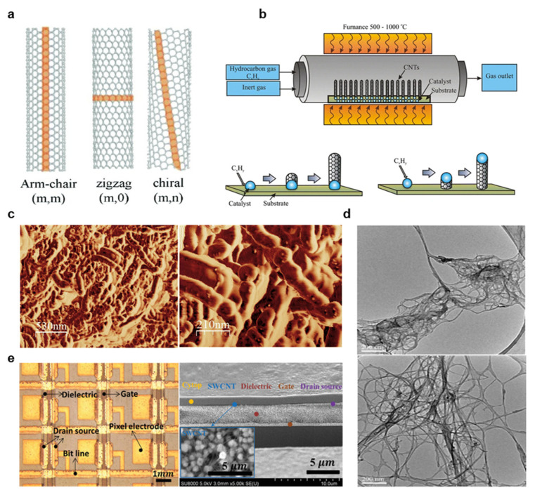
Figure 9.
Carbon nanotubes for high throughput bioelectronics printing. (a) Armchair, zigzag, and chiral CNT geometries, each of which exhibits unique material properties. (reprinted with permission from Physica E Low Dimens. Syst. Nanostruct. (2014), 59:186–191. Copyright 2014, Elsevier) (b) Schematic representation of the CVD process for CNT synthesis, with illustrations of the base growth (bottom left) and tip growth (bottom right) CNT synthesis methods. (reprinted with permission from Chem. Biol. Technol. Agric. (2016), 3(17). Copyright 2016, Springer Nature) (c) AFM images of printed MWCNTs at different magnifications. (reprinted with permission from RSC Adv. (2017), 7, 44076–44081. Copyright 2017, RSC). (d) TEM images of SWCNTs in an SDS solution after sonication for 4 h (top) and 6 h (bottom). (reprinted with permission from J. Surf. Eng. Mater. Adv. Technol. (2013), 3, 6–12. (e) Image of pixels in a roll-to-roll gravure printed TFT-active matrix with 10 PPI resolution (left) and cross-sectional FIB-SEM of printed SWCNTs on the printed dielectric (right). (reprinted with permission from Adv. Electron. Mater. (2020), 6, 1901431, Copyright 2020, Wiley).

