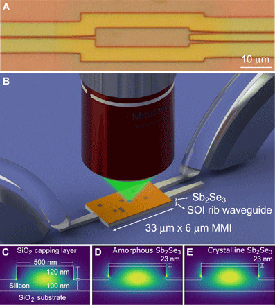
Fig. 1. Scheme showing basic principle of optically programmable silicon photonic circuits.

(A) Top view image of silicon photonic MMI. Scale bar, 10 μm. (B) Illustration of MMI with thin Sb2Se3 PCM patch and optical writing of patterns of pixels onto the device using a microscope. (C to E) Illustration of the geometry of 500-nm-wide silicon rib waveguides used in this work, without PCM patch (C) and with Sb2Se3 patch in amorphous (D) and crystalline (E) state. Simulations of the mode profile in the three cases are shown by the color map. Corresponding insertion losses between waveguide sections are shown in table S1. Photo credit: Ioannis Zeimpekis, University of Southampton.
