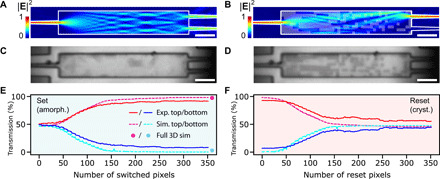
Fig. 3. Programming of an MMI 1 × 2 splitter by writing a PCM pixel pattern.

(A and B) Simulated electric field distribution for an unperturbed (A) MMI clad with 23 nm of crystalline Sb2Se3 and with a perturbed MMI with the pixel pattern of amorphous Sb2Se3 overlayed in transparent white (B). (C and D) Optical images of an experimental MMI clad with unperturbed crystalline Sb2Se3 (C) and with an amorphous pixel pattern written into Sb2Se3 (D). All scale bars, 5 μm. (E and F) Simulated transmission using 2D optimization model (green and teal dashed lines) for the top and bottom outputs of the MMI as a function of pixels written (set, amorphization) (E) and recrystallized (reset) (F) compared to the experimental values (red and blue solid lines). Dots represent final values obtained from 3D simulations with optimized pattern.
