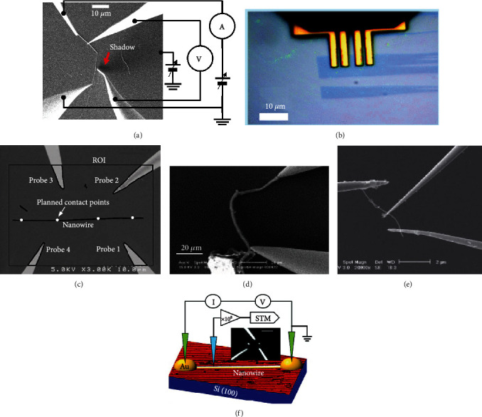
Figure 4.

SEM-based in situ electrical characterization of nanomaterials. (a) Four-point electrical transport measurement of single CNT. (b) Four-point probing of graphene flake. (c) Visual servo automated four-point probing of single nanowire. (d) Two-point electrical measurement of single nanotube by using two nanoprobes. (e) Three-point field effect measurements on CNT. (f) Three-point measurement configurations for in situ electrical transport and local density of states on a single GdSi2 nanowire.
