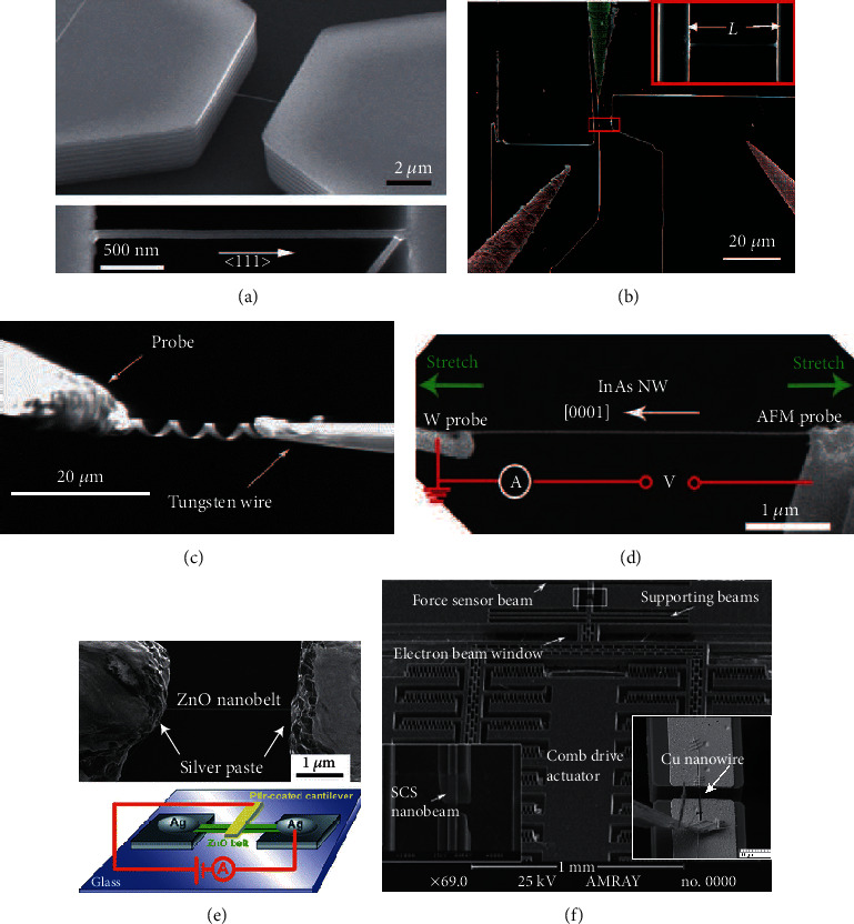
Figure 5.

Electromechanical characterization of nanomaterials. (a) Giant piezoresistance effect: single Si nanowires bridged in the trench of SOI substrate. (b) MEMS loading system for tensile testing of a suspended Si nanowire and measuring the resistance change simultaneously. (c) Conductivity measurement of deformed InGaAs/GaAs nanosprings as electromechanical sensor. (d) Electromechanical measurement of an InAs NW using a W probe and an AFM probe, the NW is uniaxially stretched, and its electrical transport properties are measured at different tensile strains. (e) SEM image of a single Sb-doped ZnO nanobelt fixed by using the silver paste and the schematic diagram of the electromechanical characterization measurements. (f) SEM image of MEMS tensile-testing chip, Cu nanowire is integrated onto the MEMS nanobeam, and its mechanical and electronic properties under different stress were characterized simultaneously.
