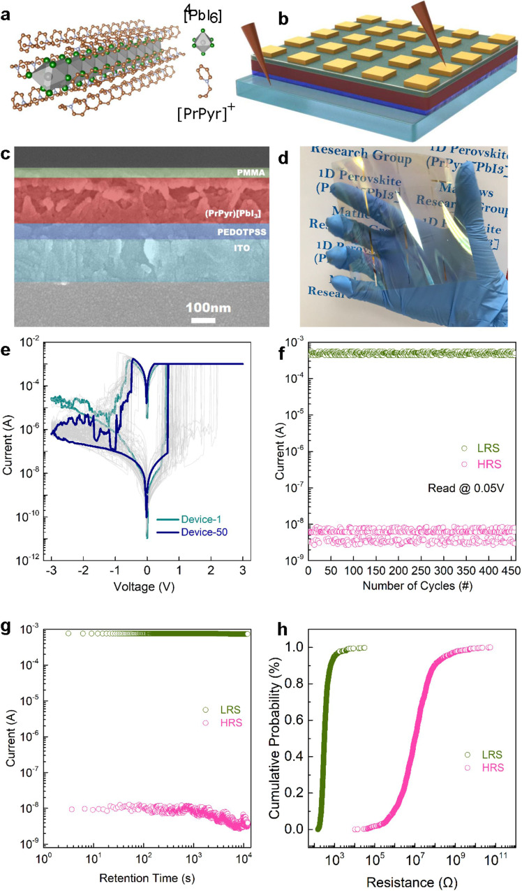
Fig. 2. 1-D Halide perovskite (HP) memristors.
a Single-crystal X-ray structure of 1-D (PrPyr)[PbI3]. Gray, green, brown and light blue spheroids correspond to Pb, I, C, and N atoms, respectively. H atoms are omitted for clarity. b Schematic and c cross-sectional scanning electron microscopy (SEM) image of the memristor device structure- Ag/PMMA/PrPyr[PbI3]/PEDOT:PSS/ITO. d Photograph of the large-area memristor array fabricated on a flexible PET substrate. e Representative DC I–V switching characteristics of HP memristors. The voltage sweeps are applied across the top Ag electrode with the bottom ITO electrode grounded. The devices switch (set) seamlessly from its high resistance state (HRS) to low resistance state (LRS) at ~+0.84 V (average of 50 devices) when the voltage is swept from 0 V→ +3 V→ 0 V. During set, a compliance current of 1 mA is applied to prevent the devices from hard breakdown. On reversing the polarity- 0 V→ − 3 V→ 0 V, the devices are reset back to their initial HRS at ~−0.51 V (average of 50 devices). f AC endurance results reflect the excellent stability of the switching process for 450 cycles. Write voltage pulses are applied to the top electrode (Vset = +1.2 V/10 ms and Vreset = −1.5 V/10 ms), followed by read pulses (Vread = 0.05 V). A read voltage of 0.05 V is chosen in order to avoid unintentional switching of the memory devices during the measurements. g Retention and h cumulative probability distribution plot of the LRS (green) and HRS (pink) across 1024 devices.

