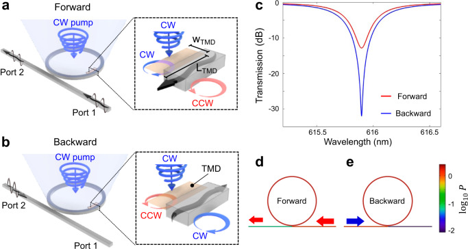
Fig. 4. All-optical isolator device design and its operation principle.
a, b SiN ring resonator loaded asymmetrically by a transition metal dichalcogenide (TMD) monolayer (on the inner side of the ring only to maximize asymmetric loss), which explains nonreciprocal transmission due to different absorption of clockwise (CW) and counter-clockwise (CCW) modes in the ring resonator. c Nonreciprocal transmission through the waveguide with forward and backward transmission shown by blue and red lines, respectively. The ring radius R = 15 μm, therefore the trip distance L = 2πR, t = 0.816, and a+ = 0.824, a_ = 0.888, which correspond to the experimentally extracted surface conductivity tensor σxx = 1.10 × 10⁻³ and σxy = 1.92 × 10⁻⁴ with parameters α = 4.69 × 10⁴ 1/m, δ = 1.13 × 10⁴ 1/m, LTMD = 3.3 μm, the width of the TMD monolayer is w = 50 nm. d, e Power density in the all-optical isolator for forward (d) and backward (e) propagating waves, respectively, as calculated from coupled mode theory (CMT).

